A PCB audit that found the boring thermal problem
The goal was simple: take a real open-source motor-driver board and ask what would matter before spinning the next revision. Not a demo schematic. Not a generic checklist. The actual board files.
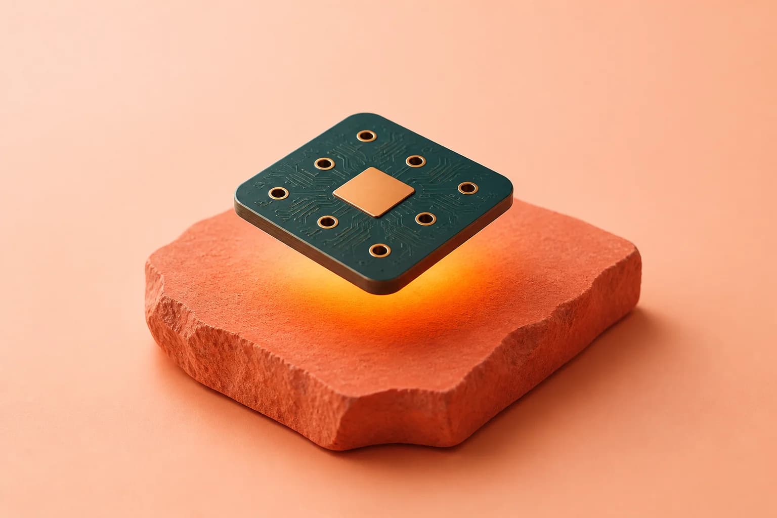
Most PCB bugs do not announce themselves as bugs. They sit quietly between the datasheet and the copper. A part looks correct. The schematic connects. The product page says a current number. Then the real board decides how much heat can leave the package.
That was the question we asked on the SimpleFOC Shield v3.2: if someone pushes this board harder, what is the first board-level thing a designer should inspect?
The useful finding was not exotic
The parser found the DRV8313 motor driver, mapped the board geometry, and checked the exposed-pad-sized thermal zone. The result was the kind of thing a hardware person can feel instantly: 0 GND vias in the PowerPAD-sized region.
That does not prove the board will fail. It does make the next revision obvious. If the motor driver is the heat source, and the board gives that heat no clean path into bottom copper, then the right first ECO is not clever. Add the thermal path, then test the derating on the bench.
No via escape in the exposed-pad zone.
Stitch the pad to bottom-side ground copper.
What the GPU run was actually for
The GPU pass was not there to make one dramatic temperature claim. It was there to make a large paired comparison cheap: baseline board versus thermal vias, wider phase copper, and the combined ECO across many ambient, airflow, current, voltage, and loss assumptions.
That matters because a single thermal number is fragile. A paired sweep is more useful for triage: when the same cases are replayed across the same design variants, the output tells you which board change deserves attention first.
- Soldered PowerPAD landConnect the exposed thermal pad to top copper.
- 6–9 filled or tented viasCarry heat through the board. Nine are illustrated.
- Bottom GND islandProvide a real copper destination, then bench-test derating.
The part people often mix up
Sensor range, driver peak behavior, and continuous board rating are three different things. The audit kept those separate. The ACS712 can measure current. The DRV8313 has its own protection behavior. The PCB still has to move heat and carry copper current in the real stackup.
That is why the output is not a single safe-at-X-amps claim. The output is better: here is the missing heat path, here is the current path to inspect next, and here is the bench test that can turn the model into a rating.
- Board model
- 47 parts / 132 tracks / 76 viasParsed board artifacts.
- PowerPAD zone
- 0 GND viasThe clearest layout issue to review.
- GPU sweep
- 33.2B cases per variantPaired baseline and ECO stress cases on 4× H100.
- Bench plan
- 5 measurement pointsDRV8313, regulator, motor terminal, sensors, and phase copper.
CUDA Monte Carlo surrogate with a separate validation sweep. Used to rank ECOs and choose bench tests, not as certified thermal signoff.
The bench test writes itself
A good audit should end with something falsifiable. This one did. Put the board in the expected enclosure or free-air setup, run current bands long enough to reach steady behavior, and watch the points that the model says should matter.
- DRV8313 package case
- L78M08 regulator tab
- TB_M1 motor terminal
- ACS712 current-sensor packages
- The narrow phase/current-sense copper path
If the DRV8313 case climbs first, the thermal-via ECO was the right thing to test. If the copper or current sensors heat first, the current-path finding moves up the list. Either way, the next board spin is no longer a guess.
What this does not claim
This is not certified PCB signoff, and the absolute temperature numbers should be treated as surrogate-model risk indicators. The strong claim is comparative and practical: from real board files, the audit found a missing thermal escape path, ranked the ECOs, and produced a bench plan that a hardware team could actually run.